|
Thin Film Solar Cells
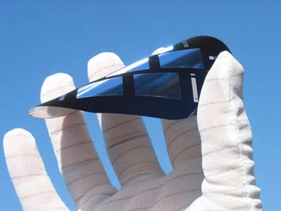
Thin film solar cells use much less light absorbing material than bulk silicon technologies. Thin film solar cells have become popular compared to wafer silicon due to lower costs and advantages including lighter weights and ease of building integration. We explore the various thin film technologies and advancements below. It gets a little technical at some points so get ready for a steep learning curve!
In the case of silicon thin films, processing costs are greatly reduced from that of bulk silicon cells. Thin film cells generally have a lower energy conversion efficiency (an average 7 to 10% efficiency) in comparison to bulk technologies. This issue has been overcome by creating multi-layer thin films which have efficiencies above those of bulk silicon wafers. Silicon Thin Film Solar Cells Silicon thin film solar cells are made by chemical vapor deposition from silane gas and hydrogen gas. This results in either: 1. Amorphous silicon (a-Si or a-Si:H) 2. Protocrystalline silicon or 3. Nanocrystalline silicon (nc-Si or nc-Si:H), also called micro-crystalline silicon. The solar cells made from these materials generally have lower energy conversion efficiency than bulk silicon cells. They are however less expensive to produce and subsequently cheaper at point of retail sale. Amorphous silicon has a higher band-gap (1.7 eV) than crystalline silicon (c-Si) (1.1 eV), which means it absorbs the visible part of the solar spectrum more strongly than the infrared portion of the spectrum. As nc-Si has about the same band-gap as c-Si, the nc-Si and a-Si can advantageously be combined in thin layers, creating a layered cell called a tandem cell. The top a-Si cell absorbs the visible light and leaves the infrared part of the spectrum for the bottom cell in nanocrystalline Si. Solutions to overcome the limitations of thin-film crystalline silicon have been recently developed. Light trapping schemes allow weakly absorbed long wavelength light to traverse the film several times significantly enhancing the absorption of sunlight in the thin silicon films. Thermal processing techniques can significantly enhance the crystal quality of the silicon and thereby lead to higher efficiencies of the final solar cells. A silicon thin film technology is being developed for building integrated photovoltaics. This will take the form of semi-transparent solar cells which can be applied as window glazing. These cells are able to double as window tinting while generating electricity... now that is pretty amazing huh!?! Cadmium Telluride Solar Cell (CdTe) A cadmium telluride is an efficient light-absorbing material for thin-film cells. Compared to other thin-film materials, CdTe is easier to deposit and more suitable for large-scale production. Despite much discussion of the toxicity of CdTe-based solar cells, this is the only technology (apart from amorphous silicon) that can be delivered on a large scale. The perception of the toxicity of CdTe is based on the toxicity of elemental cadmium, a heavy metal that is a cumulative poison. However it has been shown that the release of cadmium to the atmosphere is lower with CdTe-based solar cells than with silicon photovoltaics and other thin-film solar cell technologies. Copper-Indium Selenide (CuInSe2) The materials based on CuInSe2 that are of interest for photovoltaic applications include several elements from groups I, III and VI in the periodic table - and I am sorry but this section gets a little more technical - so here goes... These semiconductors are especially attractive for thin film solar cell application because of their high optical absorption coefficients and versatile optical and electrical characteristics which can in principle be manipulated and tuned for a specific need in a given device. CIS is an abbreviation for general chalcopyrite films of copper indium selenide (CuInSe2) and CIGS mentioned below is a variation of CIS. CIS films (no Ga) achieved greater than 14% efficiency. Manufacturing costs of CIS solar cells at present are high when compared with amorphous silicon solar cells but continuing work is leading to more cost-effective production processes. The first large-scale production of CIS modules was started in 2006 in Germany by Wuerth Solar. Manufacturing techniques vary and include the use of Ultrasonic Nozzles for material deposition. When gallium is substituted for some of the indium in CIS, the material is referred to as CIGS, or copper indium/gallium diselenide, a solid mixture of the semiconductors CuInSe2 and CuGaSe2, often abbreviated by the chemical formula CuInxGa(1-x)Se2. Unlike the conventional silicon based solar cell, which can be modelled as a simple p-n junction, these cells are best described by a more complex hetero-junction model. The best efficiency of thin film solar cells as of March 2008 was 19.9% with CIGS absorber layer. Higher efficiencies (around 30%) can be obtained by using optics to concentrate the incident light or by using multi-junction tandem solar cells. The use of gallium increases the optical band-gap of the CIGS layer as compared to pure CIS, thus increasing the open-circuit voltage, but decreasing the short circuit current. In another point of view, gallium is added to replace indium due to gallium's relative availability to indium. The atomic ratio for Ga in the >19% efficient CIGS solar cells is ~7%, which corresponds to a band-gap of ~1.15 eV. CIGS solar cells with higher Ga amounts have lower efficiency. For example, CGS solar cells which have a band-gap of ~1.7eV have a record efficiency of 9.5% for pure CGS and 10.2% for surface-modified CGS. Some investors in solar technology worry that production of CIGS cells will be limited by the availability of indium. Producing 2 GW of CIGS cells (roughly the amount of silicon cells produced in 2006) would use about 10% of the indium produced in 2004. For comparison, silicon solar cells used up 33% of the world's electronic grade silicon production in 2006. Nanosolar claims to waste only 5% of the indium it uses. That being said, indium can easily be recycled from decommissioned PV modules. Se allows for better uniformity across the layer and so the number of recombination sites in the film are reduced which benefits the quantum efficiency and thus the conversion efficiency. Gallium Arsenide (GaAs) Multi-junction Cells High-efficiency multi-junction cells were originally developed for special applications such as satellites and space exploration, but at present, their use in terrestrial concentrators might be the lowest cost alternative in terms of $/kWh and $/W. These multi-junction cells consist of multiple thin films produced using Metal-organic vapour phase epitaxy. A triple-junction cell, for example, may consist of the semiconductors: GaAs, Ge, and GaInP2. Each type of semiconductor will have a characteristic band gap energy which, loosely speaking, causes it to absorb light most efficiently at a certain color, or more precisely, to absorb electromagnetic radiation over a portion of the spectrum. The semiconductors are carefully chosen to absorb nearly all of the solar spectrum, thus generating electricity from as much of the solar energy as possible. GaAs based multi-junction devices are the most efficient solar cells to date, reaching a record high of 40.7% efficiency under solar concentration and laboratory conditions. This technology is currently being utilized in the Mars rover missions. Tandem solar cells based on monolithic, series connected, gallium indium phosphide (GaInP), gallium arsenide GaAs, and germanium Ge pn junctions, are seeing demand rapidly rise. Triple-junction GaAs solar cells were also being used as the power source of the Dutch four-time World Solar Challenge winners Nuna in 2005 and 2007, and also by the Dutch solar cars Solutra (2005) and Twente One (2007). The Dutch Radboud University Nijmegen set the record for thin film solar cell effiency using a single junction GaAs to 25.8% in August 2008 using only 4 µm thick GaAs layer which can be transferred from a wafer base to glass or plastic film. Dye-Sensitized Thin Film Solar Cells(DSSC) Typically a ruthenium metal-organic dye (Ru-centered) is used as a mono-layer of light-absorbing material. The dye-sensitized solar cell depends on a mesoporous layer of nanoparticulate titanium dioxide to greatly amplify the surface area (200-300 m2/g TiO2, as compared to approximately 10 m2/g of flat single crystal). The photo-generated electrons from the light absorbing dye are passed on to the n-type TiO2, and the holes are passed to an electrolyte on the other side of the dye. The circuit is completed by a redox couple in the electrolyte, which can be liquid or solid. This type of cell allows a more flexible use of materials, and is typically manufactured by screen printing and/or use of Ultrasonic Nozzles, with the potential for lower processing costs than those used for bulk solar cells. However, the dyes in these cells also suffer from degradation under heat and UV light, and the cell casing is difficult to seal due to the solvents used in assembly. In spite of this, DSSC is a popular emerging technology with some commercial impact forecast within this decade. Organic/Polymer Thin Film Solar Cells Organic solar cells and Polymer solar cells are built from thin films (typically 100 nm) of organic semiconductors such as polymers and small-molecule compounds like polyphenylene vinylene, copper phthalocyanine (a blue or green organic pigment) and carbon fullerenes and fullerene derivatives such as PCBM. Energy conversion efficiencies achieved to date using conductive polymers are low compared to inorganic materials, with the highest reported efficiency of 6.5% for a tandem cell architecture. However, these cells could be beneficial for some applications where mechanical flexibility and disposability are important. These devices differ from inorganic semiconductor solar cells in that they do not rely on the large built-in electric field of a PN junction to separate the electrons and holes created when photons are absorbed. The active region of an organic device consists of two materials, one which acts as an electron donor and the other as an acceptor. When a photon is converted into an electron hole pair, typically in the donor material, the charges tend to remain bound in the form of an exciton, and are separated when the exciton diffuses to the donor-acceptor interface. The short exciton diffusion lengths of most polymer systems tend to limit the efficiency of such devices. Nanostructured interfaces, sometimes in the form of bulk hetero-junctions, can improve performance. If you are still reading congratulations - you made it through the topic of thin film solar cells and all the technical talk hasn't done your head in... or it has left you spinning!! Either way now you have a much better understanding of thin film solar cells. Thin film solar cells are likely to become a standard feature in the future of building integrated solar power.
Return From Thin Film Solar Cells To Home Page |