|
The Czochralski Process
The Czochralski process is named after Polish scientist Jan Czochralski. It is the process of growing single crystals of semiconductors (e.g. silicon, germanium and gallium arsenide), metals (e.g. palladium, platinum, silver, gold), salts, and synthetic gemstones. The process was discovered in 1916 while Jan Czochralski was investigating the crystallization rates of metals.
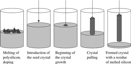
The most important application may be the growth of large cylindrical ingots, or boules, of single crystal silicon for use as semiconductors. Gallium arsenide and other semiconductors can also be grown by this method. It is usual however to obtain these semiconductors using other methods as lower defect densities obtained. How The Czochralski Process Works High-purity silicon is melted down in a crucible. A seed crystal mounted on a rod, is dipped into the molten silicon. The rod is pulled upwards and rotated at the same time. A large, single-crystal, cylindrical ingot is extracted from the melt by precisely controlling the temperature, rate of pulling and speed of rotation. The following video shows a diagram and explains the process well. Size Of Crystals While the largest silicon ingots produced today are 400 mm in diameter and 1 to 2 metres in length, 200 mm and 300 mm diameter crystals are standard industrial processes. Thin wafers are cut from these ingots of about 0.2 - 0.75 mm thick. These are polished to a very high flatness for making integrated circuits, or textured for making solar cells. The Czochralski process has played an important role in the development of solar technology.
Return From Czochralski Process To Home Page |


